Vize
- Vize için örnek sorular
Final
- Final için örnek sorular
Vize
Final
This course teaches practical data mining and big-data analytics—covering supervised/unsupervised learning, association rules, anomaly detection, and feature engineering—across text, image, and audio domains using real-world datasets. Students build end-to-end mini projects with Python (scikit-learn, PyTorch) and WEKA, and learn evaluation with ROC/PR, AUC, and explainability.
Pazartesi 19.00-22.00
Dr. Öğr. Üyesi Vecdi Emre Leven
Yok
Python
Dersin haftalık 3 saat teorik bölümü bulunmaktadır. Öğretim üyesi tarafından verilen ders materyallerinin ders öncesi incelenip, ders sonrasında ise tekrar edilmesi beklenmektedir.
Dönem içerisinde iki adet quiz yapılacaktır. 30 dk süre verilecektir. Quiz tarihi bir hafta önceden duyurulacaktır.
Derslere %80 oranında devam zorunludur.
Dönem notu; vize, lablar, ödevler, proje ve final sınavı ile belirlenecektir. Değerlendirme yüzdeleri aşağıdaki tabloda verilmiştir.
| Faaliyetler | Oranlar |
|---|---|
| Vize | %20 |
| Ödev/Quiz | %10 |
| Proje | %20 |
| Final | %50 |
Ödev ve quizlerin teslim saati üzerinden her geçen saat için 5 puan kesilecektir.
Dönem sonu notunun karşılık geldiği ağırlık ve harf notu aşağıdaki tabloda verilmiştir.
| Dönem Notu | Ağırlık | Harf Notu |
| 90-100 | 4.00 | AA |
| 85-89 | 3.50 | BA |
| 80-84 | 3.00 | BB |
| 75-79 | 2.50 | CB |
| 65-74 | 2.00 | CC |
| 50-64 | 1.50 | DC |
| 45-49 | 1.00 | DD |
| 0 -44 | 0 | FF |
Öğrencinin dönem içinde göstermesi beklenen efor tablosu aşağıda verilmiştir.
| İçerik | Saat | Kaç Defa | Ara Toplam |
| Derse Hazırlık | 2 | 14 | 28 |
| Ders Tekrarı | 2 | 14 | 28 |
| Ödev | 4 | 6 | 24 |
| Proje | 48 | 1 | 48 |
| Sınıf Dersi | 4 | 14 | 56 |
| Ara Sınav ve Final | 24 | 2 | 48 |
Öğrenciler dersten başarılı olmak için dönem boyunca ortalama 232 saat harcamaları beklenmektedir.
Kodlama ödevlerinin notlandırılması, kodun doğruluğu, kalite ve algoritmik gerçeklemedeki detayları incelenerek yapılacaktır.
Verilecek her bir ödev için test girişi ve beklenen çıkışlar paylaşılacaktır. Ancak ödev kontrolü yapılırken sizinle paylaşılmamış başka test durumları da denenecektir. Çalışma zamanı, beklenenden çok uzun süren kodlar yanlış olarak değerlendirilebilir.
Kod, istenen algoritmanın tasarımı olmalıdır. En optimum çözüm beklenmemektedir. Ancak bellek ve çalışma zamanı beklenenden çok fazla olmamalıdır.
Ödev kendi el yazınız ile yazılmalıdır. Ödev cevap kağıtının üzerinde, dersin adı, öğrenci adı ve soyadı, öğrenci numarası ve tarih bulunmalıdır.
Ödevin amacı, ders hakkında derinlemesine araştırma yapmayı öğrenmek ve pratik bilgiler kazanmayı sağlamaktır. Verilen ödevler hakkında, diğer öğrenciler ile birlikte çalışma teşvik edilmektedir. Çalışma grubu oluşturan öğrenciler, kendi başına çalışan öğrencilere göre sınavlarda daha başarılı olmaktadırlar.
Ancak bir ödevi çözmek için başkaları ile birlikte çalışsanız bile, her bir sorunun çözümünü yardım almadan kendiniz yapmalısınız. Çözümünüzü bir araştırma yolu ile elde ederseniz (örn. bir internet araması), çözümü kendi cümle ve/veya kodunuz ile ifade etmelisiniz. Çözümü sözlü olarak sorulduğunda, öğrencinin açıklayabilmesi beklenmektedir.
Verilen ödev bir kod ise, kendinizin yazması gerekmektedir. Hata ayıklamada başkalarından yardım alabilirsiniz. Kodda intihal tespiti için manuel ve otomatik mekanizmalar kullanılacaktır. İntihal, sınav içi kopya ve benzeri davranışlar disiplin yönetmeliğine göre cezalandırılır.
Course Description: This course teaches practical data mining and big-data analytics—covering supervised/unsupervised learning, association rules, anomaly detection, and feature engineering—across text, image, and audio domains using real-world datasets. Students build end-to-end mini projects with Python (scikit-learn, PyTorch) and WEKA, and learn evaluation with ROC/PR, AUC, and explainability.
Örnek Sorular:
6) Yazım İlkeleri
7) MAKALE YAZIMINDA YAPAY ZEKA ARAÇLARI VE ARAÇLAR
8) KAYNAK VERME VE YÖNETİMİ İÇİN ARAÇLAR
9) YAYININ SUNUMU
10. YAYININ DERGİLERE GÖNDERİM SÜRECİ
11. BİLİMSEL ETİK
Bu dersin amacı, öğrencilerin bilimsel araştırmayı baştan sona planlayıp yürütebilecek, bulgularını etik ilkelere uygun biçimde yazıp sunabilecek yetkinliğe ulaşmalarını sağlamaktır. Ders kapsamında bilgi ve bilim kavrayışından başlayarak araştırma sürecinin adımları, etkili literatür taraması ve stratejileri, yapay zekâ destekli tarama ve yazım araçlarının bilinçli kullanımı, veri analizi için temel araçlar, akademik yazım ve kaynak verme kuralları, kaynak yönetimi yazılımları, yayın hazırlama ve dergilere gönderim süreçleri ele alınacak; öğrenciler elde ettikleri becerileri sunumlar ve uygulamalarla pekiştirerek nitelikli bir bilimsel çalışma üretmeyi öğreneceklerdir.
Pazartesi 9.00-14.00
Dr. Öğr. Üyesi Vecdi Emre Levent,
Yok
Weka
OneNote
Dersin haftalık 3 saat teorik olarak işlenecektir
Derslere %80 oranında devam zorunludur.
Dönem notu; vize, ödevler ve final sınavı ile belirlenecektir. Değerlendirme yüzdeleri aşağıdaki tabloda verilmiştir.
| Faaliyetler | Oranlar |
|---|---|
| Vize | %30 |
| Ödev/Quiz | %20 |
| Final | %50 |
Dönem sonu notunun karşılık geldiği ağırlık ve harf notu aşağıdaki tabloda verilmiştir.
| Dönem Notu | Ağırlık | Harf Notu |
| 90-100 | 4.00 | AA |
| 85-89 | 3.50 | BA |
| 80-84 | 3.00 | BB |
| 75-79 | 2.50 | CB |
| 65-74 | 2.00 | CC |
| 50-64 | 1.50 | DC |
| 45-49 | 1.00 | DD |
| 0 -44 | 0 | FF |
Öğrencinin dönem içinde göstermesi beklenen efor tablosu aşağıda verilmiştir.
| İçerik | Saat | Kaç Defa | Ara Toplam |
| Derse Hazırlık | 2 | 14 | 28 |
| Ders Tekrarı | 2 | 14 | 28 |
| Sınıf Dersi | 4 | 14 | 56 |
| Ara Sınav ve Final | 24 | 2 | 48 |
Ödevin amacı, ders hakkında derinlemesine araştırma yapmayı öğrenmek ve pratik bilgiler kazanmayı sağlamaktır. Verilen ödevler hakkında, diğer öğrenciler ile birlikte çalışma teşvik edilmektedir. Çalışma grubu oluşturan öğrenciler, kendi başına çalışan öğrencilere göre sınavlarda daha başarılı olmaktadırlar.
Ancak bir ödevi çözmek için başkaları ile birlikte çalışsanız bile, her bir sorunun çözümünü yardım almadan kendiniz yapmalısınız. Çözümünüzü bir araştırma yolu ile elde ederseniz (örn. bir internet araması), çözümü kendi cümle ve/veya kodunuz ile ifade etmelisiniz. Çözümü sözlü olarak sorulduğunda, öğrencinin açıklayabilmesi beklenmektedir.
Verilen ödev bir kod ise, kendinizin yazması gerekmektedir. Hata ayıklamada başkalarından yardım alabilirsiniz. Kodda intihal tespiti için manuel ve otomatik mekanizmalar kullanılacaktır. İntihal, sınav içi kopya ve benzeri davranışlar disiplin yönetmeliğine göre cezalandırılır.
Ders Açıklaması: Bu dersin amacı, öğrencilerin bilimsel araştırmayı baştan sona planlayıp yürütebilecek, bulgularını etik ilkelere uygun biçimde yazıp sunabilecek yetkinliğe ulaşmalarını sağlamaktır. Ders kapsamında bilgi ve bilim kavrayışından başlayarak araştırma sürecinin adımları, etkili literatür taraması ve stratejileri, yapay zekâ destekli tarama ve yazım araçlarının bilinçli kullanımı, veri analizi için temel araçlar, akademik yazım ve kaynak verme kuralları, kaynak yönetimi yazılımları, yayın hazırlama ve dergilere gönderim süreçleri ele alınacak; öğrenciler elde ettikleri becerileri sunumlar ve uygulamalarla pekiştirerek nitelikli bir bilimsel çalışma üretmeyi öğreneceklerdir.
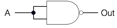
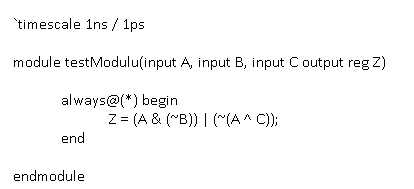
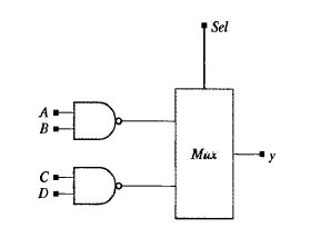
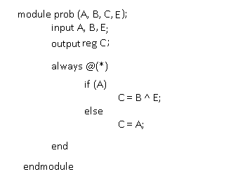
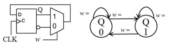
Kobinasyonel Devreler
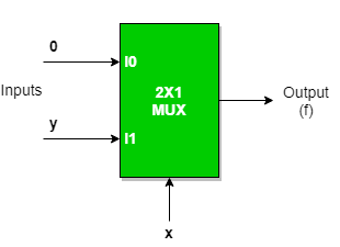
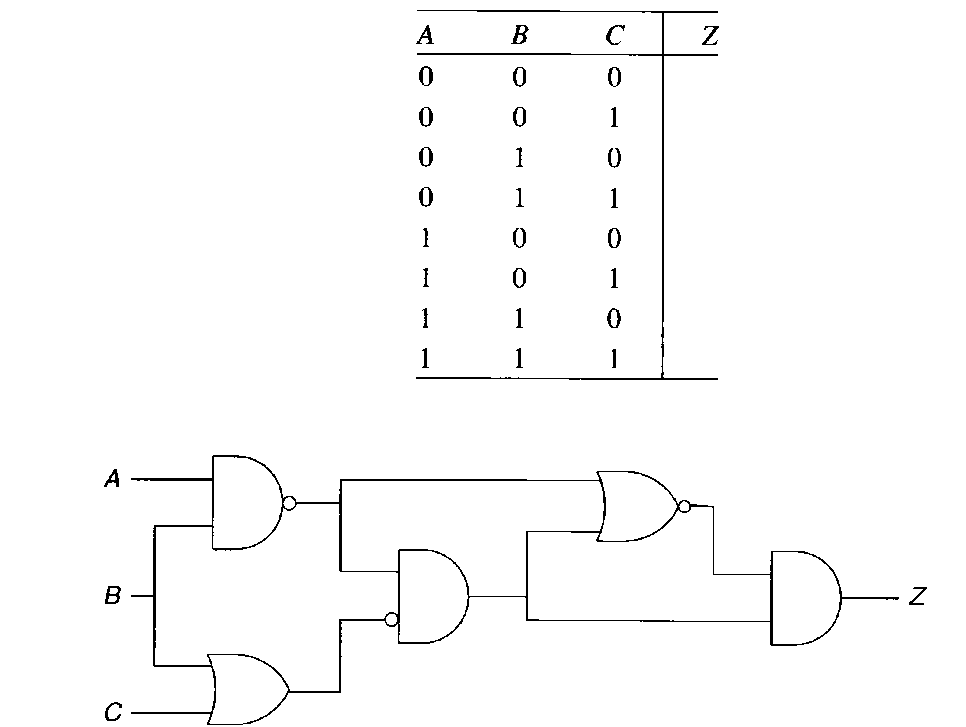
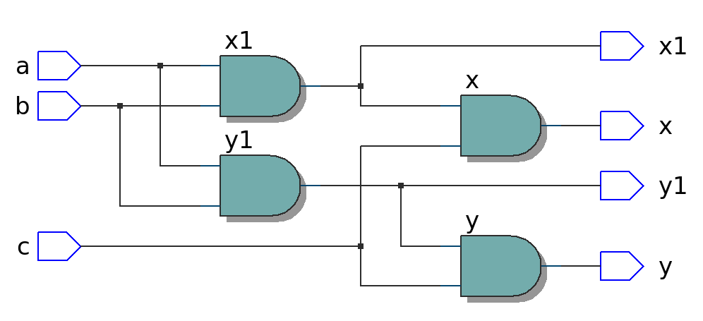
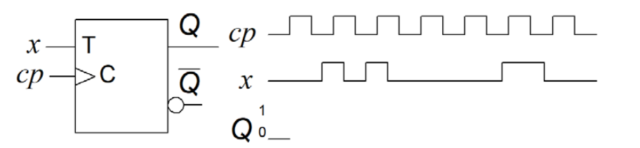
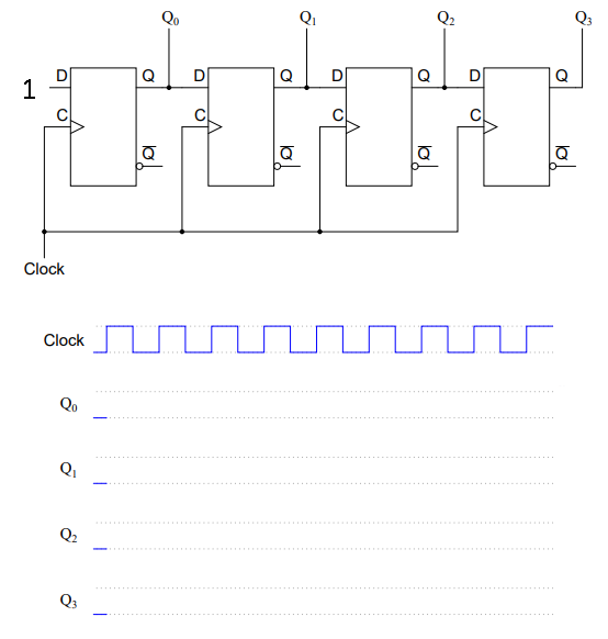
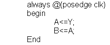
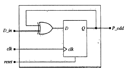
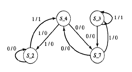
Ardışık Lojik
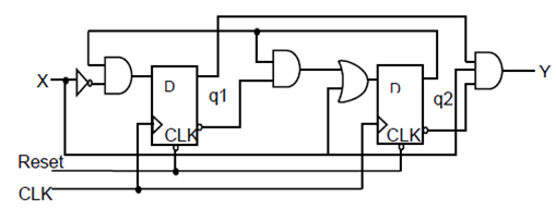
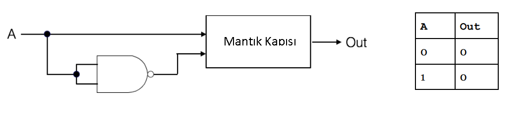
A -) 0110
B -) 1001
C -) 0100
D -) 1101
Doğrulama Yaklaşımları
Durum Makinaları
MCU Donanım Tasarımı